A closer look at the Fetzer Valve
FET booster based on a vintage Fender 12AX7 input stage
by runoffgroove.com
| This project is rated 1 out of 3 for the level of complexity. |
1. Introduction
In the two years since the Fetzer Valve was first published in the midst of our adaptation of tube amps for use as distortion pedals, the circuit has enjoyed popularity as a standalone booster and as a building block in larger circuits. While the circuit has its merits, we decided to further explore it to determine if it was a truly faithful solid-state version of the familiar input stage used in many tube amps.
The original Fetzer Valve circuit is presented in Fig.1.
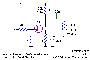
Fig.1 (Original Fetzer Valve schematic)
This circuit was developed by applying the well known Triode-to-JFET translation to the first stage found in a typical Fender tube amp, as illustrated in Fig.2.

Fig.2 (Valve to JFET transformation)
The steps involved can be summarized as follows:
Before we proceed, here are the aspects of the Fetzer Valve that will be discussed:
2. High and Low Gain Inputs
High and Low gain inputs are often noted on the faceplate as 1 and 2, respectively. Fig.3 shows the typical input circuit of a Fender tube amp. The key to understanding this circuit lies in the fact that the tip of each input jack is making electrical contact with the arrow-shaped terminal when no plug is inserted. When a plug is inserted, the contact with the arrow terminal is opened, thus interrupting this previous connection.

Fig.3 (Original Fender input stage and equivalent Hi and Low input schematics)
As shown, the Low Gain input is in fact a resistive divider that introduces 6 dB attenuation and presents a relatively low impedance to the guitar, which is 68k + 68k = 134k, hence its "Low Gain" designation. When a low impedance source is connected to the amplifier, the grid of the valve "sees" an equivalent resistance of 68k || 68k = 34k.
The High Gain input introduces no attenuation and presents a 1 Mohm impedance to the instrument. Again, a 34k equivalent resistance appears in series with the grid when a low impedance source is connected to the amplifier.
A guitar with its volume dimed will have an output impedance lower than 34k. The importance of the series resistance with the grid becomes evident in the next section.
3. Frequency Response
Fig.4 shows the simulated frequency response of the valve circuit when driven by a low impedance source, and a modified JFET stage that has a similar high frequency response. In both cases the -3 dB knee is located close to 20 kHz.

Fig.4 (Frequency response of the valve and equivalent JFET circuits)
The main purpose of the cathode capacitor (22 uF) is to boost the gain of the stage. As a side effect, the low frequency response is also affected by the value of this capacitor, however, in the Fender input stage this effect occurs well below 80 Hz.
On the other hand, the high frequency response is limited near 20 kHz, despite there is no visible capacitor capable of doing this! After a second thought, a 20 kHz bandwidth is a good thing for guitar audio, and it also prevents RF and radio stations from getting into the amp--a good thing indeed!
The phenomena responsible for determining the high frequency limit are the Miller capacitance of the triode and the equivalent resistance to the grid, 34k. The Miller capacitance corresponds to the grid-to-plate parasitic capacitance (around 4 pF for a 12AX7) times the stage gain (around 34 dB or 50 times), which gives an approximated input capacitance of 4 pF x 50= 200 pF.
Based on the aforementioned figures, the 3dB high frequency corner can be calculated as 23kHz. Now we understand the importance of the equivalent series grid resistance and why the circuit configuration was chosen to have the same value for both inputs.
Now going into the JFET equivalent circuit, we notice that most JFETs have a smaller gate-to-drain capacitance (typically in the range from 0.5 to 2 pF), and the overall gain of such a stage will be also smaller (between 6db and 26 db or 2 times to 20 times typically). Thus, it is rather inconvenient to rely on this capacitance to define high frequency limit.
A better alternative is to simply ignore the JFET's input capacitance (since it is rather small) and add an extra gate-to-GND capacitor. This extra capacitance should be around 220 pF, however any capacitor in the range from 150pF to 250pF should work appropriately.
4. Harmonic Content
It is well known that the plate voltage of a triode is related to the grid voltage by the three-halves power law, which produces both even and odd harmonics. As the signal level increases, the 2nd harmonic rises, followed by the 3rd harmonic, and then higher ordered harmonics start to appear.
On the other hand, the JFET drain current is related to the gate-to-source voltage by a square law. This means that theoretically only 2nd harmonic distortion is produced, unless the signal is strong enough to produce clipping.
In order to be faithful to the three-halves power law found in triodes, Dimitri Danyuk proposes the use of a carefully chosen source resistor on the JFET amplifier in his article "Triode Emulator" (as presented at the 116th Audio Engineering Society Convention, May 2004 in Berlin, Germany). This resistor should not be bypassed by a capacitor to produce the appropriate amount of negative feedback to change the square law of the FET into an approximation of the three-halves law of the triode.
Consider this:
a. linear circuit = unity or 1.0 exponent
b. triode = 1.5 exponent
c. JFET = 2.0 exponent
d. JFET with "magic" Rs and no bypass cap = 1.5 exponent around the operating point
In summary, for the harmonic distortion produced by a FET to have a complexity similar to a triode, the familiar 22uF source bypass cap must be omitted.
Danyuk suggests that a source resistor equal to:
Rs = 0.83 * |Vp| / Idss
will closely approximate the three-halves power law around the operating point of the JFET, where Vp is the pinch-off voltage of the JFET (a negative value for N-channel devices), and Idss is the saturation current of the device. These two parameters should be measured for the particular device in use in order to calculate the exact source resistor. In this article |Vp| represents the positive value of Vp.
Example: Consider a J201 with Vp=-0.75V and Idss=0.35mA. Then, Rs = 0.83 * 0.75V / 0.00035A = 1779 ohms. A practical standard value would be Rs = 1k8.
Example: Consider a 2N5457 with Vp=-1.5V and Idss=3mA. Then, Rs = 0.83 * 1.5V / 0.003A = 415 ohms. Practical standard values would be Rs = 390 ohms or 430 ohms.
(Notice that we used the positive value of Vp in the above calculations.)
As a general rule, JFETs with higher values of |Vp| and/or Idss will require smaller source resistors, which has the following implications to take into account:
5. Optimal Biasing
Normally, biasing of the drain voltage in JFET amplifiers is performed by adjusting the drain resistor with one of the following methods:
The proposed optimal biasing allows the largest dynamic range where the JFET approximates the three-halves law if the suggested Rs is used.
The optimum drain voltage, which is dependent on the supply voltage and Vp, can be approximated by:
Vd = 0.6*Vcc + 0.7*|Vp|
In addition, the required drain resistor can be expressed as:
Rd = 0.9 * (Vcc - 2*|Vp|) / Idss
It must be noted that normally Rd should be trimmed to comply with the Vd criteria, nevertheless, it is useful to define a starting point and eventually choose the drain trimpot with a nominal value closer to twice the anticipated Rd value for ease of adjustment.
It is useful to calculate Id in order to determine the current consumption of the Fetzer stage. This is done with the following equation:
Id = Idss * (0.44*Vcc - 0.78*Vp) / (Vcc - 2*Vp)
Finally, it is possible to also calculate the source voltage Vs as:
Vs = Vp * (0.37*Vcc - 0.65*Vp) / (Vcc - 2*Vp)
Knowing Vd and Vs in advance is useful for trimming the circuit. With the circuit powered up, adjust Rs trimmer for Vs first, then adjust Rd trimmer for Vd.
6. Input Levels
The first valve stage of a Fender amp can withstand input voltages up to +/- 2.5V without noticeable clipping.
The proposed JFET stage will start clipping when the input voltage exceeds +/- |Vp|. It is interesting to notice that the maximum input voltage without clipping is independent of Vcc and Idss. Then clipping-free input dynamic range is defined by:
Vi = +/- |Vp|
Example: A J201 with Vp=-0.75V will accept up to +/- 0.75V before entering into the clipping region.
If clipping is undesired, one of the following workarounds might be considered:
7. Stage Gain
The gain of the first 12AX7 stage in the Fender amp is near 35 dB or 50 times.
The gain of the proposed JFET stage is calculated by:
Av = 0.5 * Rd / Rs
Replacing the optimal values for Rd and Rs gain can be also expressed as:
Av = 0.54 * (Vcc/|Vp| - 2)
Some remarks on the gain formulae are:
Example: Consider a MPF102 whose Vp=-3V. If a 9V supply is used, gain will be 0.54 times or -5 dB, which is less than unity! If the supply voltage is doubled to 18V, the resulting gain will rise to 2.2 times or 7 dB!
Example: A J201 with Vp=-0.6V fed by 9V will have a gain of 7 times or almost 17 dB. (However, as we already know this stage will clip as soon as the input voltage exceeds the +/- 0.6V range.)
8. Output Dynamic Range
The drain voltage can vary from 2*|Vp| (when input voltage is +|Vp|) up to Vcc (when input voltage is -|Vp|). Thus, the output dynamic range can be expressed as:
Vo = Vcc - 2*|Vp|
Example: A 2N5458 with Vp=-2.5V will be able to swing its drain between 5V and 9V, provided that the output load resistance is much higher than Rd, meaning its output dynamic range is limited to 4V.
9. Fetzer Valve Revisited
At this point it is in order to present a circuit that incorporates the presented refinements. Fig.5 shows the schematic of the Fetzer Valve Revisited:

Fig.5 (Fetzer Valve Revisited)

Fig.6 (Fetzer Valve Revisted perfboard layout)
Pablo De Luca (aka Gringo) contributed a PCB layout for the Fetzer Valve Revisited (PDF, 178k)
The circuit can be set up according to the following steps:
Example: Assume we have a 2N5457 with measured Vp=-1.5V and Idss=3mA. The presented equations dictate the following design data if a 9V supply is to be used:
See the calculator below to determine your component values.
Choosing whether to include a source capacitor (and subsequently, the value of that capacitor) should be approached with the knowledge of how the Fetzer Valve stage will be used. Its inclusion increases gain (while reducing the clipping-free input range) while producing pure 2nd order harmonics. Having pure 2nd order harmonics is not necessarily undesirable, but different from a triode, which is the goal of the Fetzer Valve Revisited. For the cleanest possible output and closest approximation of a triode, it should be omitted. If the builder is interested in allowing some clipping in an effort to add character or wants to increase overall gain, the traditional 22u source bypass cap can be included. Or, a smaller cap can be used to accentuate certain frequencies, as illustrated with the Presence control in the Fetzer Valve Deluxe and discussed below.
Fig.7 shows the simulated waveform and harmonic distortion obtained for the Fetzer Valve using the component values from the above example. The red line shows the drain bias voltage when the input is zero.

Fig.7 (Simulated waveform and harmonic distortion of Fetzer Valve Revisited)
10. Fetzer Valve Deluxe
If a JFET with small |Vp| is used and clipping with guitar volume at maximum is not desired, a resistive attenuator might be added. This is implemented by replacing the 1Mohm input resistor with a 1Mohm LEVEL pot or trimpot. In order to avoid affecting the high frequency cutoff, the 33k input resistor and 220 pF filter cap are moved ahead of the trimpot. In this case a slight attenuation (0.28 dB) will be introduced when the LEVEL pot is dimed.
Another area open for modification is adding a cap in parallel with Rs. If a very large cap is added, the overall stage gain will increase by 6 dB, the clipping-free input range will be reduced by a similar amount, and the harmonics will be closer to the original Fetzer Valve, e.g. mostly 2nd order. A more interesting mod consists of adding a smaller cap instead, chosen to add brightness to the sound.
The value of this capacitor depends on Rs and the desired knee frequency fn, and can be calculated as:
Cp = 1 / (2*pi*Rs*fn)
where fn should be within 200 Hz and 2 kHz according to the desired effect on the mid and high frequencies. A 1 kHz corner frequency produces a nice Presence effect. This cap may be made switchable.
Example: if using a J201 with the average Vp and Idss shown in the next section and Rs= 1076 ohms, then a suitable Presence capacitor would be Cp = 1 / (2*pi*1076*1000) = 147 nF, thus, 150 nF, 120 nF or 180 nF would do fine.
A final refinement over the conventional Fetzer Valve would be to use a higher supply voltage, perhaps 12V, 15V or even 18V. This won't increase the input dynamic range but will increase the gain to allow more driving muscle out of this stage.
See the calculator below to determine your resistor and Presence capacitor values.
Fig.8 shows a Deluxe version of the Fetzer Valve Revisited.

Fig.8 (Fetzer Valve Deluxe)

Fig.9 (Fetzer Valve Deluxe perfboard layout)
Pablo De Luca (aka Gringo) contributed a PCB layout for the Fetzer Valve Deluxe (PDF, 178k)
11. Measurement of Vp and Idss
Fig.10 shows the setup required to measure Vp and Idss for an N-channel JFET.
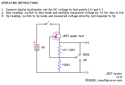
Fig.10 (Vp and Idss measurement setup)
As shown, a 9V battery, two resistors, a SPDT switch, and a DMM (digital multimeter) are required. Analog voltmeters won't work here for the Vp reading since input impedance must be at least 1 Mohm in order not to disturb the source biasing.
Follow the instructions above for Vp and Idss measurement.
The following data pertains to the specified number of JFETs we sampled for Vp and Idss. Average Rs value provides a reference starting point. Average Idss and Gain are based on a supply voltage of 9V. For ease of adjustment, you should use a trimpot that is twice the expected value of Rs and Rd. Note that in most cases the spread of values is over 2:1.
Out of ten (10) J201
average Vp: -0.83V (spanning from -0.57 to -0.97)
average Idss: 0.64mA (spanning 0.30mA to 0.83mA)
average Rs: 1076 ohms
average Rd: 10321 ohms
average Gain: 4.8 times or 13.6 dB
Out of ten (10) 2SK30AY
average Vp: -1.41V (spanning from -1.26 to -1.52)
average Idss: 2.14mA (spanning 1.78mA to 2.50mA)
average Rs: 505 ohms
average Rd: 2602 ohms
average Gain: 2.4 times or 7.6 dB
Out of twelve (12) 2N5457
average Vp: -1.58V (spanning from -1.22 to -1.80)
average Idss: 3.27mA (spanning 1.96mA to 4.11mA)
average Rs: 401 ohms
average Rd: 1607 ohms
average Gain: 2 times or 6 dB
Out of ten (10) 2N5458
average Vp: -2.18V (spanning from -1.74 to -2.87)
average Idss: 5.22mA (spanning 3.62mA to 7.41mA)
average Rs: 347 ohms
average Rd: 800 ohms
average Gain: 1.1 times or 1 dB
Out of twenty-four (24) MPF102
average Vp: -2.34V (spanning from -1.76 to -3.11)
average Idss: 5.65mA (spanning 3.91mA to 7.15mA)
average Rs: 344 ohms
average Rd: 688 ohms
average Gain: 1 times or 0 dB
Out of five (5) PN4392
average Vp: -3.64V (spanning from -3.34 to -4.10)
average Idss: 43.9mA (spanning 39.2mA to 48.7mA)
average Rs: 68.8 ohms
average Rd: 35.3 ohms
average Gain: 0.25 times or -12 dB
12. Fetzer Valve Calculator

Fetzer Valve by runoffgroove.com is licensed under a Creative Commons Attribution-NonCommercial-ShareAlike 3.0 Unported License.
Permissions beyond the scope of this license may be requested.